Professional printed wiring fabrication and design
We offer one-stop service ranging from automatic control circuit designing, electronic circuit hardware designing, PCB circuit designing, microcontroller researching and development, PC software programming, product exterior industrial designing, prototype developing, circuit board manufacturing, SMT chip enhancing, DIP welding enhancing, usability testing to aging testing etc.
Both our PCB and SMT plants have obtained certifications such as ISO9001\ISO14001\TS16949 and 3C\UL\CE\CSA\SAA\FDA for R&D and OEM products.
Strength in printed wiring fabrication and designM
(1) Comparative Advantages in printed wiring fabrication and design
Experienced printed wiring fabrication and design team - our R&D team consists of highly educated professionals with Masters and PhD degrees who are also experts in both local and international advanced technologies. Additionally, we have a group of experienced engineers who have more than 30 years behind them in circuit design. All key players in our team are skilled designers with over 10 years of experiences in microcontrollers.
Robust printed wiring fabrication and design Capability - we capitalize on our team’s vast experiences gained in product designs for different industries to provide custom-made designs offering high usability and stability at low costs.
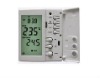
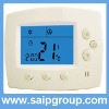
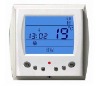
Printed wiring fabrication and design Experts - we have developed over 100 products in 30 different categories ranging from small household appliances, electromechanical equipments, packaging machines, medical equipments, body building machines, remote locking devices, RF induction devices, power modules, bioelectronics and so forth.
(2) Printed wiring fabrication and design Content
PCB Layout - our professional PCB layout engineers are highly proficient with these software applications: protel 99se, DXP2004, Altium Designer 6.0, Powerpcb5.0, Pads2007, CadSoft Eagle 5.7, Mentor WG 2004, Cadence Allegro 16.2, PCAD2004, Cadence OrCAD 10.5, cadstar 9.0, Mentor EN 2002, CR5000 9.0 that can be applied to 1-8 layers of PCB boards.
Microcontroller Programming - our microcontroller programming are compatible with these brands: Freescale, NXP, Winbond, NEC, Renesas, Fujistu, HT, Samsung, STC, Atmel, Silicon, Rabbit, Microchip, ST, TI., Infineon, Toshiba, Hynix, Sonix, etc.
Embedded Software - compatible with ARM, DSP, CPLD, FPGA etc. on embedded software development
Hardware - our years of experiences in electronic and mechanical product designs enable us to make full evaluation of the systems in terms of reliability, stability, adaptability under challenging environments and so forth. On top of that, we are skilled in the designs of highly reliable power supply, I/O signal optical isolation, dual RAM redundant, interference-free mechanism, software filtering feature and so forth.
Printed wiring fabrication and design Capability
PCB capable to produce 500,000 square feet of 2-12 layers with 4mil in sign blanks and 0.2mm in aperture per month
SMT chip 4 high-speed production lines with daily output capacity to produce 1.6 million chips that are compatible with 0402 and BGA package families in various high-precision micro component
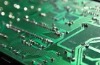
PCB Production
| Product | Single sided to 12 layers PCB |
| Material | FR1, FR2, CEM1, CEM3, FR4, BT |
| Board thickness | 0.4mm to 3.2mm |
| Base copper | H oz to 6oz |
| Min. hole size Min LW/LS | 0.3mm 0.1mm(Flash Gold)/0.15mm(HASL) |
| Aspect ratio | 1 : 6 |
| Soldermask | LPI type, Baked type, Peelable mask |
| Surface finishing | HASL, Flash gold, Immersion gold, Gold finger, Carbon ink |
| Max. panel size | 508mm x 610mm |
| Bow & twist | 0.7% (1.5mm board) |
| Hole size tol. | PTH: +/-0.08mm, NPTH: +/-0.05mm |
| Hole location tol. | +/-0.05mm |
| Gold thickness | 0.05um to 1.5um |
| Nickel thickness | 1um to 5um |
PCBA Touchups
1 Objectives
Producing PCBA control panels by following PCB diagrams, component checklists, burning processes and testing methodologies provided by clients
2 Specifications
can accommodate chips components containing 0402 and above and high-precision components such as BGA etc.
chip speed of 0.015S/ chips
chip precision ≥0.01 mm
3 Output capacity
4 Japanese JUKI high speed chip production lines consist of 1 automated printer, 2 high speed chip machines, 1 multi-purpose chip machine and 1 reflow machine.
Daily output of 160,000 chips
Expert of PCB and PCBA control circuit board OEM and ODM